What Is CoWoS? TSMC's Advanced Packaging and the AI Chip Bottleneck
An AI accelerator is not one chip but several: a large processor and stacks of high-bandwidth memory, joined in one package. TSMC's CoWoS is the packaging that most of them use. Here is how it works, why TSMC said it could not meet demand, and where new capacity is going.
The chips that train and run AI models are not single pieces of silicon. An AI accelerator such as Nvidia’s is a large processor surrounded by stacks of high-bandwidth memory (HBM), and the processor and the memory have to sit very close together, in one package, so that data can move between them fast enough. Joining them is a manufacturing step of its own, called advanced packaging. For Nvidia’s and AMD’s accelerators, that packaging is TSMC’s CoWoS. Nvidia’s latest annual report says simply: “We utilize CoWoS technology for semiconductor packaging.”
What does CoWoS stand for?
CoWoS stands for Chip on Wafer on Substrate, and the name describes the layers:
- Chip: the processor dies and the HBM stacks.
- On wafer: they are mounted side by side on an interposer, a thin layer that carries thousands of fine connections between them. In the original version the interposer is cut from a silicon wafer.
- On substrate: the interposer, with its chips, is mounted on a package substrate that connects to the circuit board.
TSMC calls this “advanced 2.5D packaging technology.” The chips sit next to each other rather than on top of one another, which is why it is 2.5D and not 3D. In TSMC’s words, “by integrating multiple SoCs and high-bandwidth memory stacks, CoWoS empowers products with high-performance compute and memory bandwidth.” The technology is not new: TSMC says it has been in volume production since 2012.
What are the three versions?
TSMC lists three, which differ in what the interposer is made of:
| Version | Interposer | TSMC’s notes |
|---|---|---|
| CoWoS-S | A large silicon interposer holding logic chiplets and HBM | Interposers “up to 3.3X-reticle size (or ~2700mm2)” |
| CoWoS-R | A redistribution layer (RDL) interposer of polymer and copper traces | In volume production since 2023 |
| CoWoS-L | An RDL interposer with embedded local silicon interconnect (LSI) bridges | First 3.5X-reticle version in volume production since 2024 |
The “reticle” is the area that a lithography tool can pattern in one go, so a 3.3X-reticle interposer is more than three times the size of the largest single chip. Bigger interposers let more processor dies and more HBM stacks fit in one package. On its October 15, 2026 earnings call, TSMC said it was the only one at 5x reticle and was working on 9x and 14x.
CoWoS is one of three families TSMC groups as 3DFabric: SoIC, which TSMC describes as “a wafer-level 3D IC chip stacking platform”; InFO, a wafer-level packaging technology with “a high-density redistribution layer (RDL)”; and CoWoS.
Why do AI chips need it?
The answer is memory bandwidth. HBM is DRAM built as a stack of chips:
- Micron calls it “a high-performance, 3D-stacked DRAM designed to deliver massive data throughput for AI.”
- SK hynix describes “vertically stacked DRAM chips using Through Silicon Via (TSV),” optimized “for deep learning accelerators and AI systems.”
- Samsung says its HBM uses TSV-based stacking “to accelerate AI training and HPC workloads.”
Each HBM stack is wired to the processor through the interposer, over a very short distance and with many fine connections. The standards body JEDEC published the HBM3 standard in January 2022 and HBM4 in April 2025.
The pattern holds beyond Nvidia. AMD wrote in December 2024 that its MI300X accelerators “leverage advanced 3.5D CoWoS packaging” with “192GB of high-bandwidth memory (HBM3).” Who Makes What in Memory covers the HBM makers.
Why did CoWoS become a bottleneck?
Because demand for AI accelerators outran the packaging capacity. TSMC’s own earnings calls show it:
- January 16, 2025: TSMC described “very tight capacity” that could not “even meet customers’ need.”
- April 17, 2025: “We are also working hard to double our CoWoS capacity in 2025,” TSMC said; CEO C.C. Wei described demand as “almost insane” and the capacity as “still fully loaded.”
- January 15, 2026: TSMC said advanced packaging contributed slightly over 10% of its revenue in 2025, up from about 8% in 2024, and that it expected a low-teens percentage in 2026. Revenue from AI accelerators was a high-teens percentage of its 2025 revenue.
By TSMC’s own account, packaging capacity was a limit on how much it could supply. The shift shows in TSMC’s revenue mix, where the high-performance computing (HPC) platform has taken a larger share:
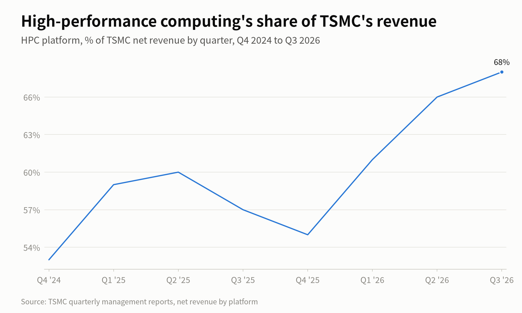
TSMC’s third-quarter 2026 report put HPC at 68% of net revenue and smartphones at 21%. For the full-year mix by platform, see Foundry, Fabless and IDM.
Where is CoWoS made?
Most of TSMC’s advanced packaging is in Taiwan, and new capacity is being built there and in the US:
- Zhunan, Taiwan: Advanced Backend Fab 6, which TSMC opened in June 2023 as “TSMC’s largest advanced backend fab to date,” with capacity of more than a million 12-inch wafer equivalents a year.
- Taichung, Taiwan: Advanced Backend Fab 5, in the Central Taiwan Science Park.
- Southern Taiwan Science Park: TSMC’s 2025 annual report lists land leases for two more advanced backend fabs, AP7 and AP8.
- Arizona, US: in March 2025 TSMC announced plans for “two advanced packaging facilities” as part of its US expansion, which its Arizona page now puts at US$265 billion. The page says construction of the first advanced packaging fab began in early 2026.
- Peoria, Arizona (Amkor): in October 2024 TSMC and Amkor said TSMC would contract packaging and test services, including CoWoS and InFO, from Amkor’s planned plant there. The US CHIPS program awarded Amkor up to US$407 million for the roughly US$2 billion project, and Amkor’s filings say construction began in the second half of 2025.
TSMC is not the only company offering this kind of packaging. ASE Technology, the Taiwanese packaging and test company, lists “2.5D/FO-MCM/FO-EB/CoWoS” among its own solutions in its annual report, and TSMC named Intel’s EMIB-T as a competing approach on its October 2026 call.
Where do the capacity signals come from?
CoWoS capacity is rarely published as a number. The signals come from companies’ own words and results: TSMC’s quarterly calls and its revenue by platform, the HBM makers’ statements about supply, and AI chip companies’ comments on how much they can ship. TSMC’s Monthly Sales explains the monthly revenue reports that arrive between those calls.
Sources
- CoWoS (3DFabric technology page)
- Advanced Packaging Services (TSMC 3DFabric)
- TSMC-SoIC (3DFabric technology page)
- InFO (3DFabric technology page)
- TSMC quarterly results and management reports, 4Q24 to 3Q26 (net revenue by platform; earnings conference call transcripts)
- TSMC Celebrates the Opening of Advanced Backend Fab 6 (June 8, 2023)
- TSMC fab locations
- TSMC annual report (Form 20-F) for 2025
- TSMC Intends to Expand Its Investment in the United States to US$165 Billion (Form 6-K, March 4, 2025)
- TSMC Arizona
- Amkor and TSMC to Expand Partnership and Collaboration on Advanced Packaging in Arizona (Form 6-K, October 2024)
- CHIPS incentives award to Amkor Technology (December 20, 2024)
- Amkor quarterly report (Form 10-Q), second quarter 2026
- NVIDIA annual report (Form 10-K), fiscal 2026
- Accelerating Energy Efficiency: Our Latest 30x25 Update (December 10, 2024)
- ASE Technology annual report (Form 20-F) for 2025
- High Bandwidth Memory (HBM)
- HBM
- HBM
- JEDEC Publishes HBM3 Update to High Bandwidth Memory (HBM) Standard (January 27, 2022)
Related reading
More in Explainers
- Chip Stock Heatmap Explained: How to Read the Asia-Pacific Chips MapMarket Map
- Asia Chip Stocks From a US Account: SKHY, TSM, KXIAY and Other TickersExplainers
- Who Makes What in Memory: DRAM, NAND and HBM Across Asia and the USExplainers
- How to Buy Japanese Chip Stocks: Tokyo Shares, OTC ADRs and ETFsGuides
- How to Buy Taiwan Stocks From Abroad: TWSE Shares, TSM and ETFsGuides
- What Do 3nm and 2nm Mean? Chip Process Nodes ExplainedExplainers
- US Chip Export Controls on China, ExplainedExplainers
- Foundry, Fabless and IDM: How Chipmakers Split the WorkExplainers
- Why Samsung Reports Earnings Twice, and How Other Chipmakers ReportExplainers
- SOXX vs SMH vs SOXQ: How Three Semiconductor ETFs DifferExplainers
- How a Stock Gets Into the S&P 500 and the Nasdaq-100Explainers
- Dow, S&P 500 and Nasdaq: What Each US Stock Index MeasuresExplainers
- US Stock Futures Overnight: What Dow, S&P 500 and Nasdaq Futures ShowExplainers
- One Chip Day, Four Closes: Seoul, Taipei, Tokyo and New YorkExplainers
- Japan's Margin Trading Data: What It Says About KioxiaExplainers
- Kioxia Outside Japan: 285A in Tokyo vs KXIAY Over the CounterExplainers
- Kioxia's 3-for-1 Split: How to Read Its Price HistoryExplainers
- Micron's Fiscal Calendar: Why Its Quarters Don't Match Samsung'sExplainers
- Nikkei 225 vs TOPIX: Why Chip Stocks Move Them So DifferentlyExplainers
- The Philadelphia Semiconductor Index (SOX) and Why Asia Watches ItExplainers
- Taiwan's 10% Daily Price Limit and Other Rules for Foreign InvestorsExplainers
- TSM vs 2330: Why TSMC's US Shares Trade Above TaipeiExplainers
- TSMC's Monthly Sales: How Taiwan's Monthly Revenue Reports WorkExplainers
- Why One Stock Moves Taiwan's Market: TSMC and the TAIEXExplainers
- How Foreign Investors Move the KOSPI, and Where to See the Daily DataExplainers
- How to Buy Korean Stocks in 2026: 4 Routes for US, Singapore, UKGuides
- How to Buy Samsung Stock Outside Korea: Shares, London GDR and ETFsGuides
- Korea Discount and the Value-up Program, Explained SimplyExplainers
- KOSPI Heatmap Explained: How to Read Korea's Market MapMarket Map
- Why MSCI Still Hasn't Upgraded Korea, and What Would Change ItExplainers
- How Samsung and SK hynix Compare in HBMSamsung & SK hynix
- SKHY vs 000660: How the Two Ways to Own SK hynix DifferSamsung & SK hynix
- Why Is the KOSPI So Volatile? Chips, Foreign Money and the WonExplainers