What Do 3nm and 2nm Mean? Chip Process Nodes Explained
Chipmakers name each new manufacturing generation with a number of nanometers, and the number keeps falling. It no longer measures anything on the chip. Here is what the names do mean, where TSMC, Samsung, Intel and Rapidus stand, and how much of TSMC's business each node now is.
Every year or two, chipmakers announce a new manufacturing generation with a smaller number in front of “nm”: 7nm, 5nm, 3nm, 2nm. The numbers suggest something on the chip shrinking by that many nanometers, a nanometer being a billionth of a meter. They used to mean that. They no longer do.
What does the “nm” in a node name measure?
Nothing specific, by the industry’s own account. Intel’s 2021 fact sheet on its new process names put it plainly: “For decades, the process ‘node’ name corresponded to the actual length of certain physical transistor features. While the industry departed from that practice many years ago,” the naming and numbering schemes used across the industry “no longer refer to any specific measurement.” Intel added that its own node numbers “do not represent the actual dimension of any physical feature on a transistor.”
The IEEE’s International Roadmap for Devices and Systems (IRDS), which the industry uses to map out future chip technology, goes further. Its 2022 summary says the naming “has led to a complete detachment between IC features and technology nodes’ names,” and its 2023 report notes there is “not yet a consensus on the node naming across different foundries” and chipmakers.
So a node name is best read as a generation label. Within one company, each new label means denser, faster or more power-efficient chips than the one before. TSMC’s annual report describes its leading-edge technologies as ones that “further enhance chip performance, reduce power consumption, and decrease chip size.” Across companies, the same number does not mean the same thing.
Why did Intel rename its nodes?
Because its names made its processes look a generation behind rivals whose chips were comparable. In 2021 Intel moved to “a new naming structure based on key technical parameters including performance, power and area.” What it had called 10nm Enhanced SuperFin became Intel 7, and what it had called 7nm became Intel 4. It named the step after that 20A, “to evoke the angstrom era,” an angstrom being a tenth of a nanometer.
Where does each chipmaker stand?
| Company | Node | Status, in the company’s words |
|---|---|---|
| TSMC | N3 (3nm) | “In 2022, TSMC became the first foundry to move 3nm FinFET (N3) technology into high-volume production” |
| TSMC | N2 (2nm) | “Started volume production in 4Q25,” its first nanosheet transistors |
| Samsung | 3nm | Started production on June 30, 2022, with gate-all-around (GAA) transistors it calls MBCFET |
| Samsung | SF2 (2nm) | “Started mass production in 2025” |
| Intel | Intel 18A | “First went into high-volume manufacturing in late 2025” |
| Rapidus | 2nm | Pilot line in Chitose, Hokkaido, since April 2025; “mass production is scheduled to begin in 2027” |
The newer nodes also change the transistor itself. For years the leading design was the FinFET, in which the current-carrying channel is a raised fin. At 2nm, TSMC, Samsung and Intel all move to gate-all-around transistors, in which the gate wraps the channel on all sides; TSMC calls its version nanosheets and Intel calls its version RibbonFET. Intel’s 18A also adds PowerVia, which Intel describes as “backside power delivery,” moving power wiring to the back of the wafer.
Each company also claims firsts in its own way: Samsung for the first GAA production at 3nm, Intel for GAA and backside power in high-volume manufacturing, and Samsung’s Exynos 2600 page for the industry’s first 2nm GAA mobile processor. Those are each company’s claims.
How much of TSMC’s business is at each node?
TSMC reports its wafer revenue by node every quarter, which shows how fast a new generation takes over.
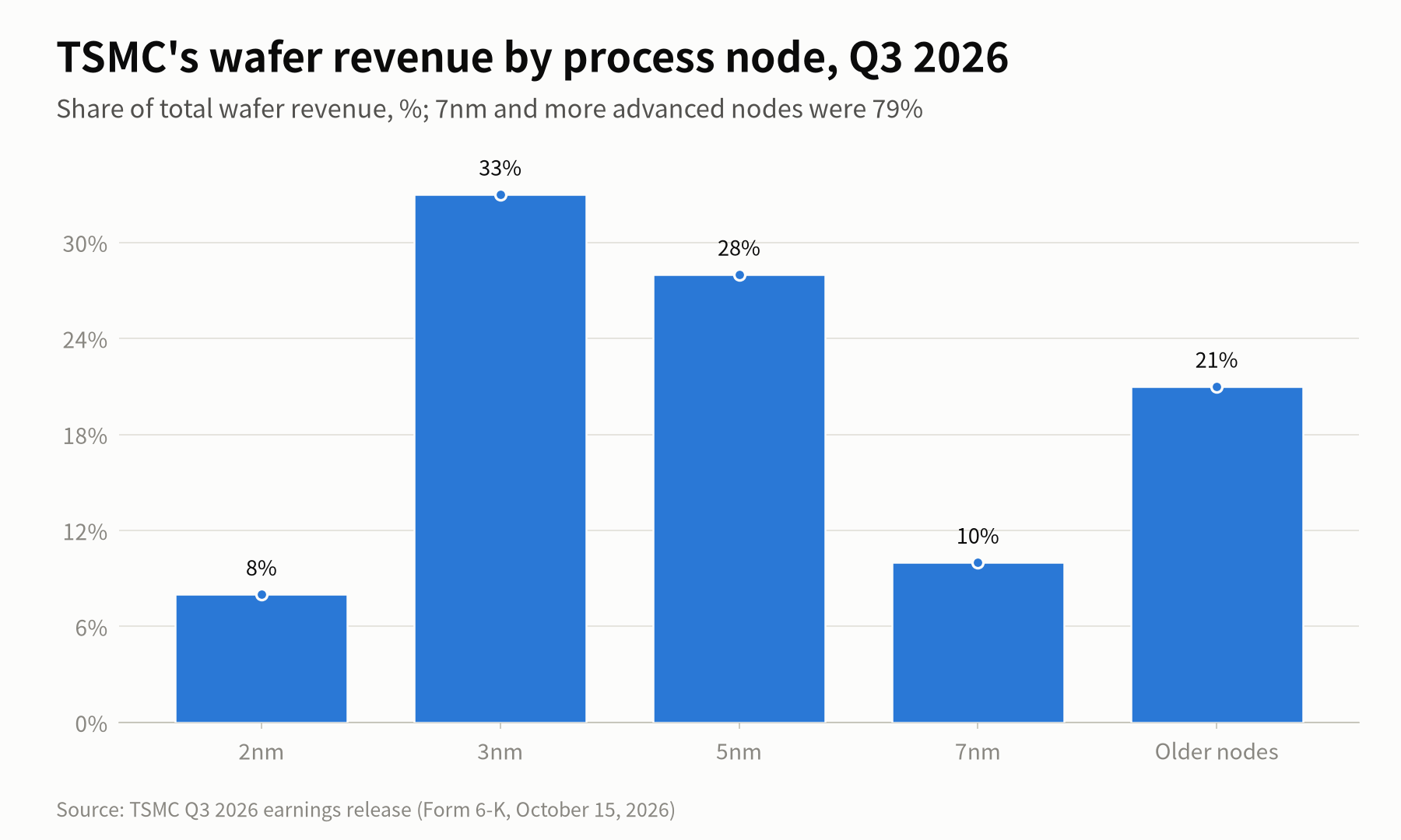
In the third quarter of 2026, 2nm, in its first year of volume production, was already 8% of TSMC’s wafer revenue, and 3nm was the largest single node at 33%. For the whole of 2025, TSMC reported 3nm at 24%, 5nm at 36% and 7nm at 14%, with nodes of 7nm and below at 74%. By the third quarter of 2026 that share had reached 79%.
What comes after 2nm?
The names move to angstroms. TSMC lists:
- A16, which adds a backside power rail. TSMC says that compared with its N2P process, A16 will give “an 8-10% speed improvement” at the same voltage or “a 15-20% power reduction at the same speed,” and that it “will be production-ready in 2H26.” Its annual report says risk production is expected in 2026.
- A14, “scheduled for volume production for 2028,” which TSMC says will give a 10-15% speed improvement or 25-30% lower power compared with N2.
- A13, scheduled for 2029.
Intel’s next step after 18A is Intel 14A, which uses High-NA EUV lithography, according to its annual report.
How is the smallest patterning done?
With extreme ultraviolet (EUV) lithography, which prints patterns with light at a wavelength of 13.5 nanometers. ASML’s annual report says EUV is used “for the most intricate, critical layers on the most advanced microchips,” and that ASML is “currently the world’s only manufacturer of EUV lithography systems.” It expects its next-generation High-NA machines to start supporting high-volume manufacturing in 2027.
What does a node name tell a reader?
That it marks a company’s generation, not a size. A 2nm chip from one company and a 2nm chip from another can differ, and a company’s own comparisons, such as TSMC’s percentages for A16 against N2P, are the clearest guide to what each step adds. For which companies design chips and which manufacture them, see Foundry, Fabless and IDM; for how the newest chips are packaged, see What Is CoWoS?.
Sources
- Accelerating Process Innovation (Intel Accelerated fact sheet, July 26, 2021)
- International Roadmap for Devices and Systems (IRDS) 2022, Executive Summary
- IRDS 2023, More Moore
- 3nm Technology
- 2nm Technology
- A16 Technology
- TSMC Unveils Next-Generation N2 Process Technology (June 16, 2022)
- TSMC annual report (Form 20-F) for 2025
- TSMC Q3 2026 earnings release (Form 6-K exhibit 99.1, October 15, 2026)
- Samsung Begins Chip Production Using 3nm Process Technology With GAA Architecture (June 30, 2022)
- Logic node (process technology)
- Intel annual report (Form 10-K), fiscal 2025
- Rapidus
- ASML annual report (Form 20-F) for 2025
Related reading
More in Explainers
- Chip Stock Heatmap Explained: How to Read the Asia-Pacific Chips MapMarket Map
- Asia Chip Stocks From a US Account: SKHY, TSM, KXIAY and Other TickersExplainers
- Who Makes What in Memory: DRAM, NAND and HBM Across Asia and the USExplainers
- How to Buy Japanese Chip Stocks: Tokyo Shares, OTC ADRs and ETFsGuides
- How to Buy Taiwan Stocks From Abroad: TWSE Shares, TSM and ETFsGuides
- US Chip Export Controls on China, ExplainedExplainers
- What Is CoWoS? TSMC's Advanced Packaging and the AI Chip BottleneckExplainers
- Foundry, Fabless and IDM: How Chipmakers Split the WorkExplainers
- Why Samsung Reports Earnings Twice, and How Other Chipmakers ReportExplainers
- SOXX vs SMH vs SOXQ: How Three Semiconductor ETFs DifferExplainers
- How a Stock Gets Into the S&P 500 and the Nasdaq-100Explainers
- Dow, S&P 500 and Nasdaq: What Each US Stock Index MeasuresExplainers
- US Stock Futures Overnight: What Dow, S&P 500 and Nasdaq Futures ShowExplainers
- One Chip Day, Four Closes: Seoul, Taipei, Tokyo and New YorkExplainers
- Japan's Margin Trading Data: What It Says About KioxiaExplainers
- Kioxia Outside Japan: 285A in Tokyo vs KXIAY Over the CounterExplainers
- Kioxia's 3-for-1 Split: How to Read Its Price HistoryExplainers
- Micron's Fiscal Calendar: Why Its Quarters Don't Match Samsung'sExplainers
- Nikkei 225 vs TOPIX: Why Chip Stocks Move Them So DifferentlyExplainers
- The Philadelphia Semiconductor Index (SOX) and Why Asia Watches ItExplainers
- Taiwan's 10% Daily Price Limit and Other Rules for Foreign InvestorsExplainers
- TSM vs 2330: Why TSMC's US Shares Trade Above TaipeiExplainers
- TSMC's Monthly Sales: How Taiwan's Monthly Revenue Reports WorkExplainers
- Why One Stock Moves Taiwan's Market: TSMC and the TAIEXExplainers
- How Foreign Investors Move the KOSPI, and Where to See the Daily DataExplainers
- How to Buy Korean Stocks in 2026: 4 Routes for US, Singapore, UKGuides
- How to Buy Samsung Stock Outside Korea: Shares, London GDR and ETFsGuides
- Korea Discount and the Value-up Program, Explained SimplyExplainers
- KOSPI Heatmap Explained: How to Read Korea's Market MapMarket Map
- Why MSCI Still Hasn't Upgraded Korea, and What Would Change ItExplainers
- How Samsung and SK hynix Compare in HBMSamsung & SK hynix
- SKHY vs 000660: How the Two Ways to Own SK hynix DifferSamsung & SK hynix
- Why Is the KOSPI So Volatile? Chips, Foreign Money and the WonExplainers