Is Samsung Handing a Key HBM Chip to TSMC?
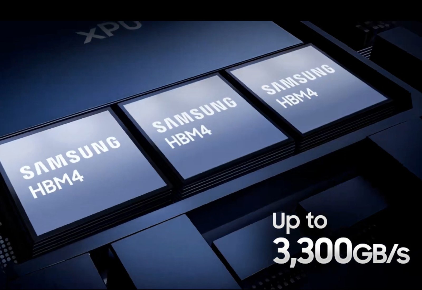
Samsung Electronics has decided to make the bottom chip (the base die) of its custom HBM for Nvidia on TSMC’s 3nm process, according to a report. HBM is the stacked high-bandwidth memory used alongside AI chips. The report says Nvidia asked all three of its suppliers, Samsung, SK hynix and Micron, to use the same process.
The Seoul Economic Daily first reported it on October 18. Reuters added that it would be the first time Samsung has teamed up with TSMC at the HBM manufacturing stage. However, none of Samsung, Nvidia or TSMC has officially confirmed it.
What does the HBM base die do?
It is the “brain” chip at the bottom of the DRAM stack
HBM is memory made by stacking several DRAM chips vertically. The stacked DRAM chips are called core dies, and the single logic chip at the very bottom is called the base die.
The base die does not store data. It acts as a guide between the AI chip and the memory, passing signals back and forth and distributing power.
NVHBM moves the memory controller into the base die
On August 26, Nvidia unveiled NVHBM, its custom HBM. It moves the memory controller, which used to sit inside the AI chip, into the base die. As a result, the base die has to be made on an advanced logic process rather than a memory process.
These are the figures Nvidia gave, compared with standard HBM4E:
- Up to 30% more memory bandwidth per stack
- Up to 15% lower HBM power consumption
- Up to 25% more AI chip area freed for compute
All of these are targets Nvidia announced, and volume shipments are expected in 2027. NVHBM was introduced for custom AI chips that use Nvidia’s chip-connection technology, NVLink Fusion.
Why did Samsung choose TSMC over its own foundry?
Nvidia asked all three suppliers for the same process
According to the report, Nvidia asked all three companies to standardize on TSMC’s 3nm process for the base die and a sixth-generation (1c) process for the DRAM stacked on top. Making the product the same way at every supplier keeps performance consistent and means it only has to be validated once.
The gap in yields is also cited as a reason. TrendForce, citing industry estimates, put TSMC’s 3nm yield at over 90% and Samsung Foundry’s 2nm yield at about 60%.
Until now, Samsung has made its own base dies
- Samsung: makes the base die for HBM4, which went into mass production this year, on its own 4nm process
- SK hynix: announced a partnership with TSMC on the HBM4 base die in April 2024
A “turnkey” approach, with one company making everything from memory to logic, has long been seen as a strength unique to Samsung. The report says Samsung is not abandoning it. Samsung will keep making standard HBM and custom HBM for other customers such as AMD in house, and it is also considering using Samsung Foundry’s 2nm process as a backup if TSMC’s capacity falls short.
To see whether the report showed up in share prices, I indexed both companies’ shares to September 1 = 100.
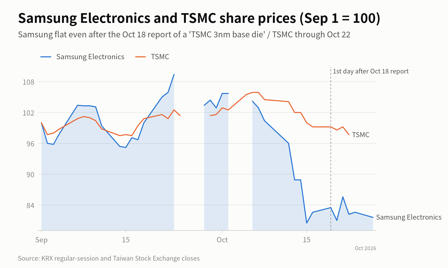
Samsung Electronics shares did not move much after the report. They were nearly flat, at 215,500 won on October 16 and 213,000 won on October 26. The shares were shaken more by the broad chip sell-off in mid-October than by this report.
What does it mean for competition in memory and foundry?
Companies with advanced foundries gain more say
As HBM’s brain becomes an advanced logic chip, the industry is moving toward a structure where even memory makers cannot make HBM without a foundry.
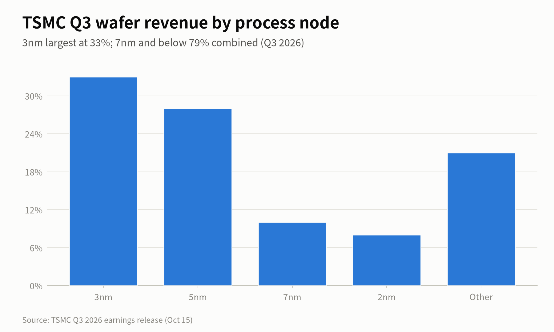
TSMC reported third-quarter results on October 15. Revenue was 1.4942 trillion New Taiwan dollars, up 50.9% from a year earlier, and net income rose 68.7%. The 3nm process made up 33% of wafer revenue, the largest share.
The contest in HBM shifts to the stacked DRAM
If the base die is the same at all three companies, the difference comes down to the DRAM stacked on top. Yields, stacking technology and heat management become the deciding factors.
HBM is also taking up more production capacity. On September 29, Samsung Electronics Executive Vice President Kim Tae-woo said HBM’s share of the industry’s DRAM wafer capacity would grow from about 20% now to close to 30% next year. Since HBM and standard DRAM share the same wafers, this means supply of standard DRAM could get tight.
Three things to watch
- Whether Samsung and Nvidia confirm the report with an official announcement
- Whether SK hynix and Micron have also accepted the same terms
- Whether Samsung Foundry’s 2nm process is actually named as a backup supplier
This post is based on reports published through October 27, 2026, and is not investment advice.
Frequently asked questions
Q1. Does this mean Samsung Foundry lags behind TSMC?
A1. It is hard to say that for certain. According to the report, this is the result of Nvidia asking all three suppliers for the same process, and Samsung is reported to be continuing to make its other HBM and other customers’ volumes at its own foundry.
Q2. Does this affect ordinary consumers too?
A2. It could, indirectly. Some expect that if HBM takes up more DRAM wafers, supply of standard DRAM for PCs and smartphones could shrink. Whether that actually shows up in prices depends on market conditions.
Sources: Reuters and TrendForce (October 19, 2026), citing the Seoul Economic Daily’s report (October 18, 2026); Nvidia’s NVHBM announcement (August 26, 2026); TSMC’s third-quarter earnings release (October 15, 2026); Reuters on Executive Vice President Kim Tae-woo’s remarks (September 29, 2026); share prices: KRX and Taiwan Stock Exchange regular-session closes. Lead photo: Samsung Electronics / Samsung Semiconductor website
Information only, not investment advice.
Related reading
More in Blog
- Caterpillar as an AI Stock: Why Midterm Data Center Curbs Hit It
- US Chip Stocks Rebound, but AI Leaders Win Back the Least
- The SOX Plunge: 3 Reasons Only Chips Fell After the Midterms
- Chip Stocks Tonight: Three Things to Watch as AMD Reports
- After the SOX Plunge: Three Checkpoints for This Week
- AI Spending Over Earnings: 3 Reasons TSMC Shares Slipped
- Why Kioxia Disappointed After Earning 2 Trillion Yen in Three Months
- The KOSPI's Roller Coaster Won't Stop. Is the Nikkei on It Too?
- SanDisk's 4.6x Revenue Outlook: What It Signals for Kioxia